20-f-003
Disclaimer:
As a condition to the use of this document and the information contained therein, the SWGDE requests notification by e-mail before or contemporaneous to the introduction of this document, or any portion thereof, as a marked exhibit offered for or moved into evidence in any judicial, administrative, legislative or adjudicatory hearing or other proceeding (including discovery proceedings) in the United States or any Foreign country. Such notification shall include: 1) the formal name of the proceeding, including docket number or similar identifier; 2) the name and location of the body conducting the hearing or proceeding; 3) subsequent to the use of this document in a formal proceeding please notify SWGDE as to its use and outcome; 4) the name, mailing address (if available) and contact information of the party offering or moving the document into evidence. Notifications should be sent to secretary@swgde.org.
It is the reader’s responsibility to ensure they have the most current version of this document. It is recommended that previous versions be archived.
Redistribution Policy:
SWGDE grants permission for redistribution and use of all publicly posted documents created by SWGDE, provided that the following conditions are met:
- Redistribution of documents or parts of documents must retain the SWGDE cover page containing the disclaimer.
- Neither the name of SWGDE nor the names of contributors may be used to endorse or promote products derived from its documents.
- Any reference or quote from a SWGDE document must include the version number (or create date) of the document and mention if the document is in a draft status.
Requests for Modification:
SWGDE encourages stakeholder participation in the preparation of documents. Suggestions for modifications are welcome and must be forwarded to the Secretary in writing at secretary@swgde.org. The following information is required as a part of the response:
- Submitter’s name
- Affiliation (agency/organization)
- Address
- Telephone number and email address
- Document title and version number
- Change from (note document section number)
- Change to (provide suggested text where appropriate; comments not including suggested text will not be considered)
- Basis for change
Intellectual Property:
Unauthorized use of the SWGDE logo or documents without written permission from SWGDE is a violation of our intellectual property rights.
Individuals may not misstate or over represent duties and responsibilities of SWGDE work. This includes claiming oneself as a contributing member without actively participating in SWGDE meetings; claiming oneself as an officer of SWGDE without serving as such; claiming sole authorship of a document; use the SWGDE logo on any material or curriculum vitae.
Any mention of specific products within SWGDE documents is for informational purposes only; it does not imply a recommendation or endorsement by SWGDE.
Table of Figures
Figure 1. Example of a Host Controller (HC) 05 Bluetooth® module pinout
Figure 2. Bluetooth® HC-05 module with soldered leads
Figure 3. Bluetooth® module connected to development board and breadboard
Figure 4. AT commands and responses
Figure 5. USB to UART Bridge
Figure 6. Connections to RN
Figure 7. Connection between module and computer via COM8
Figure 8. Terminal Setup configuration
Figure 9. Log Settings
Figure 10. Adjusting baud rate
Figure 11. Placing the module in Command Mode
Figure 12. Example of the “D” Get command
Figure 13. Module’s response from the “Y” command
Figure 14. Module response showing firmware version
Figure 15. USB driver installation
Figure 16. RN42 module pinout
Figure 17. FT232 with soldered wires
Figure 18. Module connected to FT232 through breadboard
Figure 19. Selecting FT232 in BlueFlash
Figure 20. Successful connection to BlueFlash
Figure 21. Saving extraction
Figure 22. Pairing name
Figure 23. Mac address via SPI
Figure 24. MAC address of connected computer
Figure 25. MAC address via chip-off
Figure 26. Carving Example
1. Purpose
From IOT devices to credit card skimmers, Bluetooth® modules are used as a way to wirelessly connect devices. The modules contain identifiers of devices to which they were paired / connected. The purpose of this test method is to provide specific procedures required to recover those identifiers.
2. Scope
This document is intended for computer forensic practitioners conducting embedded device forensic examinations. Reference data is available, at a minimum, in the following publications:
- SWGDE Best Practices for Examining Magnet Card Readers;
- ASTM E3017-19 Standard Practice for Examining Magnetic Card Readers;
- SWGDE Test Method for Skimmer Analysis – Analog Devices;
- SWGDE Test Method for Skimmer Analysis – Digital Devices;
- SWGDE Best Practices for Chip Off;
- SWGDE Best Practices for Computer Forensics Acquisitions; and
- SWGDE Embedded Device Core Competencies.
3. Limitations
Bluetooth® Modules present unique examination challenges due to:
- Rapid changes in technology;
- Multiple data formats; and
- Lack of commercially available software to analyze data extracted from skimmers.
4 Extraction and Analysis
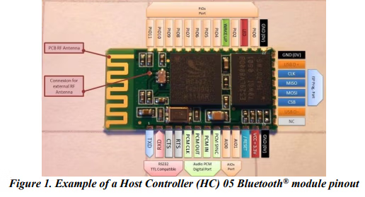
Bluetooth® module data may be extracted and analyzed in a few different ways. The process selected by the examiner will be module dependent. However, the first step to a successful examination is to locate information for the particular module that includes a pinout of external connections (see Figure 1).
Once the pinout data is known, a development board is chosen. The development board will act as an interface between the module and the examination computer facilitating the transfer of data.
4.1 Arduino
Arduino is an open source development board that allows for small amounts of software, termed a “sketch” to be uploaded to the Arduino in order to accomplish desired tasks, in this case gather information from a Bluetooth® module. The sketch also contains the mechanical connection instructions and terminal settings instructions such as baud rate in addition to the programming code; a new or edited sketch can be created by the examiner if necessary, e.g. unsupported module. Once connected from the module to the Arduino and from the Arduino to a computer via USB, the examiner uses terminal software to transmit commands and receive data over the serial communications port established between the development board and the examination computer.
Arduino Integrated Development Environment (IDE) Version 1.8.2 is the terminal software used in this example, other serial terminals include PuTTY, RealTerm, and Tera Term. As there is no logging function available within Arduino IDE, the examiner should use screen capture software to record the session.
From within the Arduino software, the examiner:
4.1.1 Opens the sketch that matches the Bluetooth module;
4.1.2 Matches the com setting as reported by the operating system device manager;
4.1.3 Uploads the sketch from the examination computer to the Arduino.
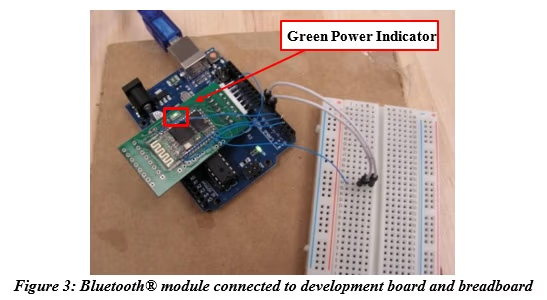
4.1.4 The examiner then makes the physical connections to the transmission, reception, ground, and power (including power to the Key pin when present) pins on the If power is not applied to a present Key pin, the device powers to broadcast mode, i.e. mode that enables pairing. Only when the examiner applies power to both the VCC (power supply pin) and Key pins, does the module enter “Command Mode”, the mode needed to later communicate with the device without overwriting former pairing data. Once in Command Mode, the green light on the module will blink approximately every two seconds (versus a rapid flashing of the light which signifies broadcast mode).
In the following example, the examiner is instructed via a sketch to connect the module to a development board
(Arduino® Uno R3) by connecting leads as follows:
- 4.1.4.1 Module transmit data (TXD) to Arduino® pin 2;
- 4.1.4.2 Module receive data (RXD) to Arduino® pin 3;
- 4.1.4.3 Module Key (PI011) to Arduino® pin 4;
- 4.1.4.4 Module VCC to Arduino pins 5 and 6 (multiple connections to a single pin can be facilitated with the use of a breadboard) to Arduino® pins 5 & 6;
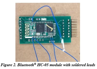
- 4.1.4.5 Module ground to Arduino®ground. See Figure 2 and Figure 3 for example connections.
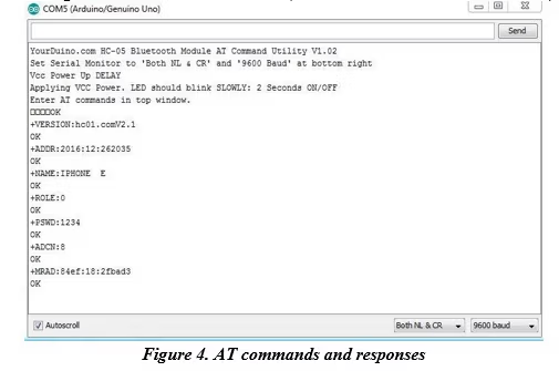
4.1.5 Within the software, the examiner opens the terminal and confirms a valid Command Mode serial connection by typing “AT” in the serial command If the device replies “OK” then the command mode serial connection is valid.
4.1.6 Once connected, the examiner can use the following commands to collect module artifacts. See Figure 4 for examples of AT commands and responses.
- 4.1.6.1 “AT+VERSION?” – Responds with software version
- 4.1.6.2 “AT+ADDR?” – Responds with the Bluetooth® module address
- 4.1.6.3 “AT+NAME?” – Responds with the Bluetooth® name (default is HC-05)
- 4.1.6.4 “AT+ROLE?” – Responds with device role (“0” is slave, “1” is master)
- 4.1.6.5 “AT+PSWD?” – Responds with pairing code (default is 1234)
- 4.1.6.6 “AT+ADCN?” – Responds with the authenticated device count (i.e. 6 or 8)
- 4.1.6.7 “AT+MRAD?” – Responds with the Bluetooth® address of the most recently authenticated device
- 4.1.6.8 “AT+FSAD=” – One can search for an authenticated device in the paired list by entering a known Bluetooth® address (“OK” = success or “FAIL” = failure)
4.1.7 The queries and responses are captured and entered into the examiner’s report.
4.2 UART
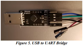
Different Bluetooth® modules may require different command sets. Using the example of a Roving Networks™, RN-41/42, a different interface to the examination computer and a different set of commands can be used. Instead of the Arduino used in the above example, the examiner may use an interface such as the USB to UART bridge pictured below.
4.2.1 To begin, the examiner sources a pin out diagram of the module, identifies and connects leads to the power, ground, TX (transmission) and RX (receive) pads. In order to make the soldered connections stronger, one may add hot glue.
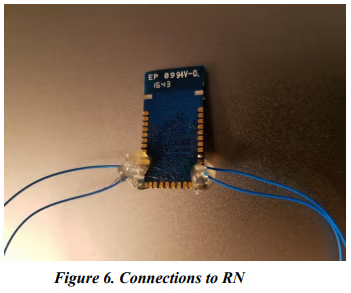
4.2.2 The examiner then connects the power and ground leads from the module to the interface board; however, TX from the module is connected to RX on the board, RX from the module is connected to TX on the board.
4.2.3 The examiner connects the interface board to his/her computer.
4.2.4 The examiner notes within the operating system’s device settings, g. Device Manager within a Windows® operating system, what serial communication port is assigned to the interface bridge.
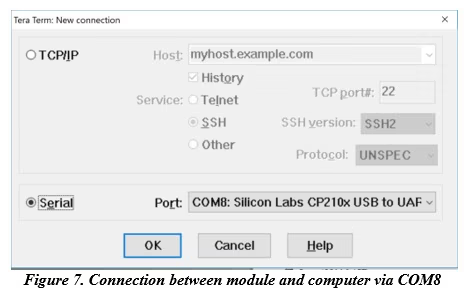
4.2.5 The examiner starts the development software, in this example Tera Term™, initiates a new connection, and selects the matching communication port (see Figure 7).
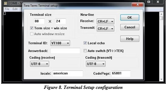
4.2.6 Within “Terminal Setup” (see Figure 8) the examiner chooses CR (carriage return) and LF (line feed) for receiving and This is done so the terminal will move the cursor down and to the beginning of the next line every time the ‘enter’ key is pressed. This is needed in order to send a command to the device. Additionally, the examiner chooses “Local echo” in order for the terminal to print to the screen what the examiner types. This is needed in order to verify commands are being typed correctly.
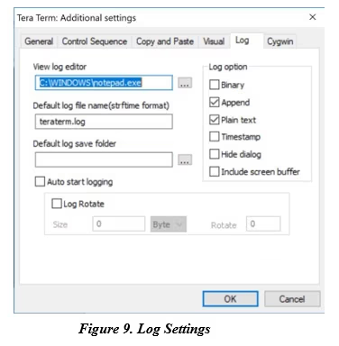
4.2.7 The examiner then ensures logging is turned on by configuring the settings and providing a path to an output file.
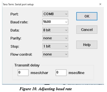
4.2.8 The examiner then confirms the correct serial port communication speed is set by adjusting the baud rate if necessary. In this example, the correct rate is 9600.
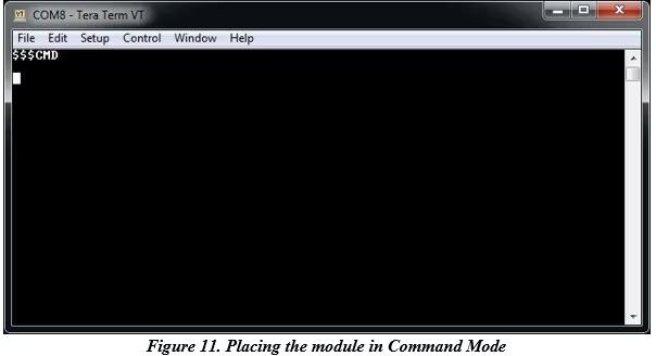
4.2.9 The examiner then places the module into command mode by entering “$$$” into the terminal window. If successful, the terminal will respond, “CMD” (see Figure 11).
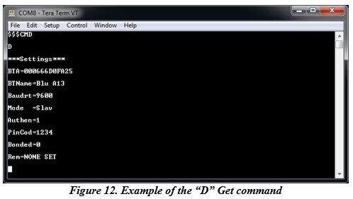
4.2.10 The examiner continues by entering “Get” A sample of commands and what they retrieve is as follows:
- 4.2.10.1 “D” – Displays basic settings such as the device Bluetooth® address, name, universal asynchronous receiver/transmitter (UART) settings, security, pin code, bonding, and remote address (Default settings are slave mode and pin code 1234, see Figure 12.)
- 4.2.10.2 “E” – Displays the extended settings such as the service name, service class, device class, and configuration timer
- 4.2.10.3 “GB” – Returns the device’s Bluetooth® address
- 4.2.10.4 “GF” – Returns the Bluetooth® address of the currently connected device
- 4.2.10.5 “GR” – Returns the stored remote Bluetooth address for re-connecting (if set)
- 4.2.10.6 “GK” – Returns the device’s current connection status (“1,0,0” indicates the device is connected; “0,0,0” indicates the device is not connected.)
- 4.2.10.7 “G<char>” – Displays the stored settings for a set command, where <char> is a set command name
- 4.2.10.8 “$$$” – Causes the device to enter command mode, displaying “CMD”
- 4.2.10.9 “—” – Causes the device to exit command mode, displaying “END”
- 4.2.10.10 “H” – Displays a list of commands and their basic syntax
- 4.2.10.11 “V” – Displays the firmware version
4.2.11 The examiner then inserts the log of the queries and module responses within his/her report.
4.3 SPI
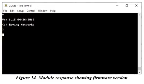
In the example above, one may notice that a possibly important artifact is not available. The last connected device (MAC address) is not listed. This is because for this particular module, the command that would have pulled that artifact (the “Y” command) is not available via UART until firmware version 6.3. Unfortunately, RN modules with firmware version 6.15 are commonly used. The “GF” command will only provide the last connected MAC until a module power cycle. See Figure 37 and Figure 38 for responses to the “Y” and “V” commands.

Another option for the examiner is to extract information from the module using the SPI protocol. Data extracted via SPI, or through chip-off (covered later in this document), allows for the analysis of a write protected binary image.
4.3.1 SPI Extraction
In order to complete an extraction via SPI, the examiner must first source and load SPI libraries onto a FT232 serial adapter board. This can be accomplished through the use of a USB driver installation tool, such as Zadig, pictured in Figure 15.
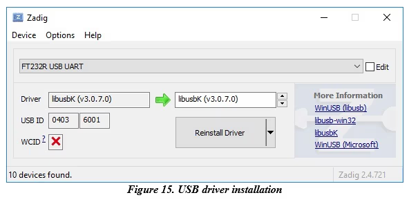
- 4.3.1.1 The examiner connects the FT232 board to an examination computer, then within the Zadig software, chooses the FT232 board in the top drop down menu, uses the up/down arrows to choose the libusbK (v3.0.7.0) driver in the right side of the window, and presses “Reinstall Driver”.
4.3.2 With the FT232 board prepared, the examiner’s next step is to source the pinout for the Bluetooth® module to be examined; in this example, the Roving Networks The pinout for the RN42 with highlighted pins that correspond with the SPI protocol for data extraction is pictured in Figure 16. Note: the pin labelling is shown from the top while the mechanical connections are made to the pads underneath the module.
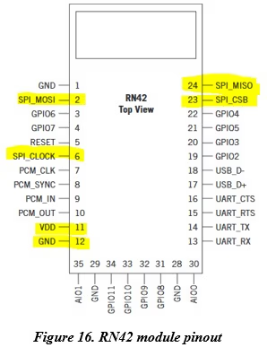
4.3.3 Continuing, the examiner must match the SPI pins (plus power and ground) of the module to the correct pins on the FT232. The connections are as follows:
DSR/RSD = MISO
RI = MOSI
RTS = CLK
DTR = CSB
3.3V = VDD GND = GND
Figure 17 shows wires soldered to the appropriate FT232 board pads. Note: The jumper should be set to 3.3. volts. The alternative, 5 volts, could damage the Bluetooth® module.
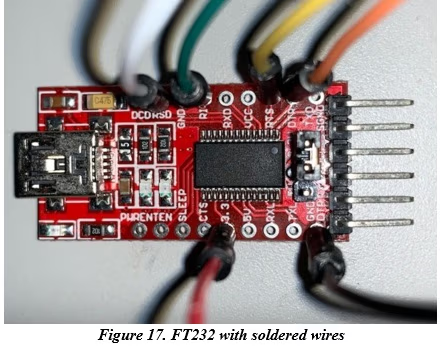
A bread board may be used to facilitate the connections between the two wire sets. Doing so relieves some of the torque that is placed on the pads that occurs if the wires are connected directly from module to FT232 board.
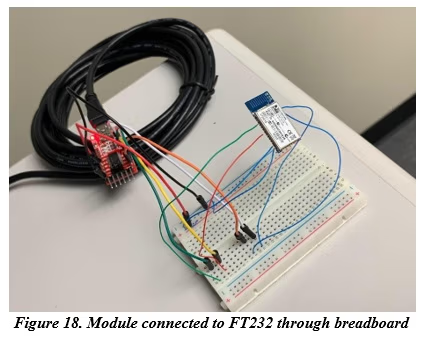
4.3.4 With the module connected to the FT232 board through a breadboard and the FT232 board connected via USB to an examination computer, the examiner then uses a software application to extract the module’s contents. In this example, a program called BlueFlash is used.
- 4.3.4.1 Using BlueFlash, the examiner chooses the FT232 board using the drop down This is shown in Figure 19.

- 4.3.4.2 Once selected, BlueFlash will attempt to recognize the Bluetooth® module’s processor. If successful, BlueFlash will report that the module is recognized and will provide size data of the module’s flash storage. The examiner then selects “Stop Processor”. This step is required for the software to complete a read of the module’s flash With the processor stopped, the examiner hits the “Dump” button. A screenshot of the BlueFlash software showing these available selections is shown in Figure 20.

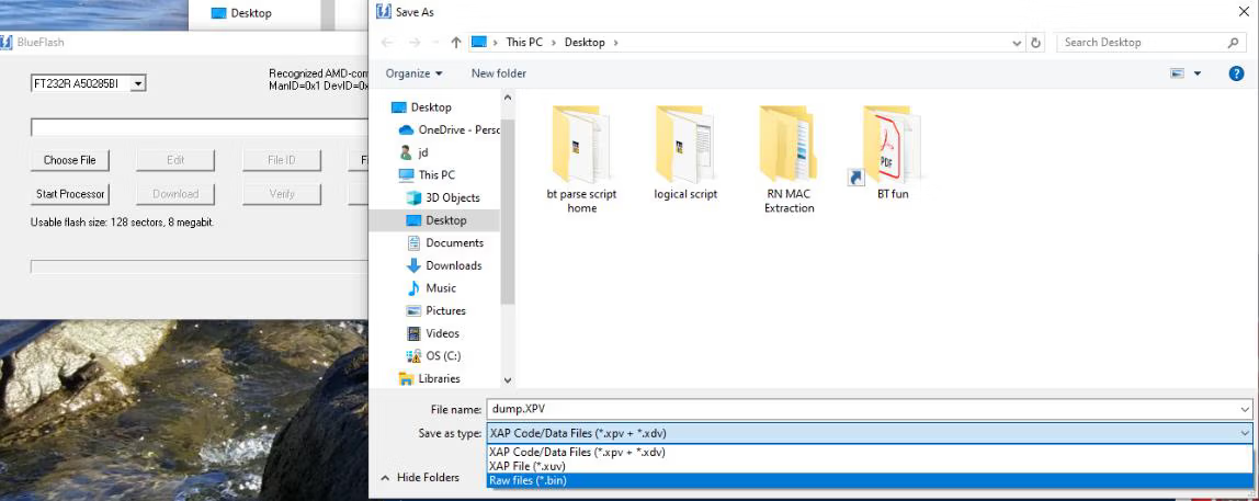
- 4.3.4.3 The examiner is given the option of saving the extraction in a couple of formats. To facilitate efficient carving, the examiner should use the “Raw files” option in order to save the extraction as a binary file. The process for saving the extraction as a binary file is shown below in Figure 21.
4.3.5 SPI Extraction Analysis
Regarding analysis of the extraction, artifacts such as the Bluetooth® pairing name is observable when opening the extraction in a hex editor. A pairing name, RNBT – FB28, in 8bit ASCII/Unicode is shown in Figure 22.
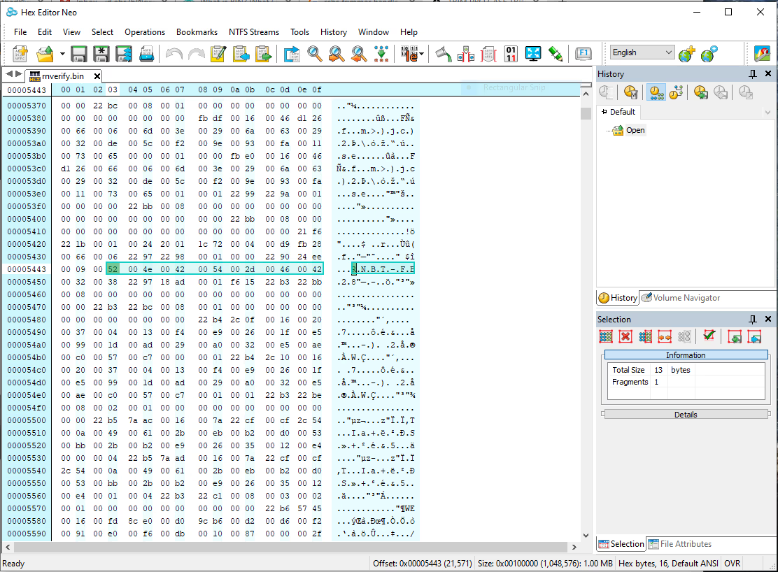
4.3.6 The recovery of connected Bluetooth® addresses is more Figure 23 shows a MAC address, but it is encoded in a way that is not immediately apparent.
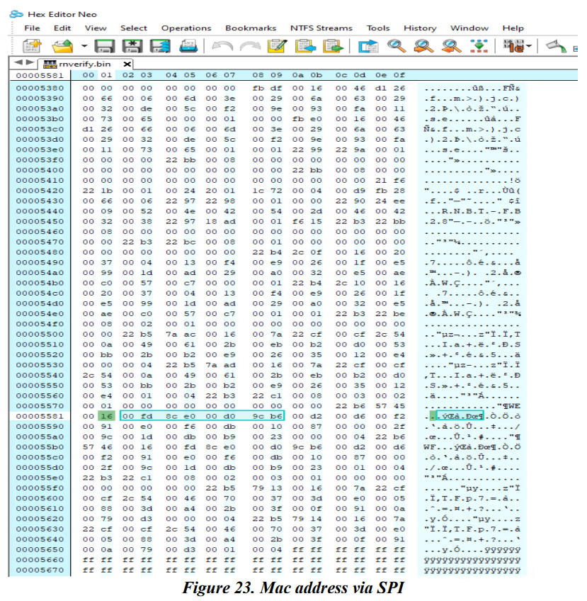
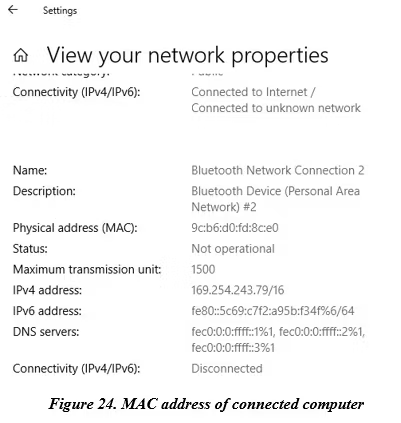
4.3.7 The hexadecimal values highlighted above: 16 00 fd 8c e0 00 d0 9c b6, represent the MAC address: 9c b6 d0 fd 8c e0, as confirmed in the test computer that paired with the The test computer’s network properties are displayed in Figure 24.
4.3.8 The format for the extracted address, 16 00 fd 8c e0 00 d0 9c b6, is as follows:
- 1st byte, 0x16 = serves as a header
- 2nd byte, 0x00 = padding
- 3rd byte, 0xfd = the fourth byte of the address
- 4th byte, 0x8c = the fifth byte of the address
- 5th byte, 0xe0 = the sixth byte of the address
- 6th byte, 0x00 = padding
- 7th byte, 0xd0 = the third byte of the address
- 8th byte, 0x9c = the first byte of the address
- 9th byte, 0xb6 = the second byte of the address
- Resolving to the MAC address of 9c:b6:d0:fd:8c:e0.
- The encoding uses the Bluetooth® address structure:
- 2 bytes of Non-significant Address Part (NAP);
- 1 byte of Upper Address Part (UAP); and.
- 3 bytes of Lower Address Part (LAP).
- However, organized as LAP, UAP, and NAP and in Big Endian.
4.4 Chip-off Analysis
While the pairing name is still viewed in close proximity to paired device MAC address, the formatting of the Bluetooth® address is a little different. Figure 25 shows data from the same module but from a chip-off extraction.
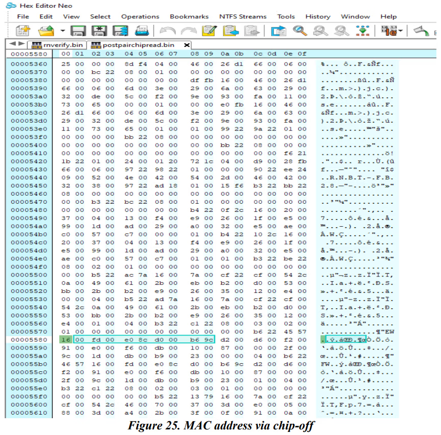
4.4.1 The format for the address, 16 00 fd 00 e0 8c d0 00 b6 9c, is as follows:
- 1st byte, 0x16 = serves as a header
- 2nd byte, 0x00 = padding
- 3rd byte, 0xfd = the fourth byte of the address
- 4th byte, 0x00 = padding
- 5th byte, 0xe0 = the sixth byte of the address
- 6th byte, 0x8c = the fifth byte of the address
- 7th byte, 0xd0 = the third byte of the address
- 8th byte, 0x00 = padding
- 9th byte, 0xb6 = the second byte of the address
- 10th byte, 0x9c = the first byte of the address
- Resolving to the MAC address of 9c:b6:d0:fd:8c:e0.
- Once again, the extraction shows the module in the LAP UAP NAP; however, it is presented as Little Endian.
5 Automation
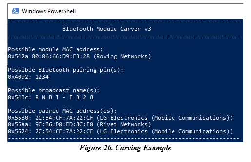
As data resident on the tested modules included addresses, pairing codes, and broadcast names not entirely from seeding events, the Endian-ness, record identifiers, and device specific headers, e.g. 0x16 for an RN module, must be factored into any artifact carving solution. Similar to other devices, e.g. drones, it is presumed that manufacturers seed data to test function before shipping to distributors. Figure 26 shows an example of a scripted carving solution.
History
| Revision | Issue Date | Section | History |
|---|---|---|---|
|
Draft |
01/22/2020 |
All |
Initial draft for public comment. |
|
DRAFT 1.0 |
01/22/2020 |
All |
Formatted and technical edit performed for release as a Draft for Public Comment. |
|
Draft 1.1 |
8/27/2020 |
All |
Technical edits. |
|
1.1 |
9/17/2020 |
All |
Voted for release as final publication |
Version: 1.1 (September 17, 2020)